
The first wall tiles and bottom blanket structure of the nuclear fusion device must simultaneously withstand high heat flux, particle bombardment and strong neutron irradiation environment. Reduction activated ferrite martensitic (RAFM) steels have been extensively researched and developed for use in the construction of first wall tiles and blankets. However, extreme operating temperatures and radiation environments pose challenges to existing RAFM steels. These challenges stem from the poor performance of existing RAFM alloys above 550°C, reduced high-temperature creep-brittle strength, and radiation-induced embrittlement. Castable Nanostructured Alloys (CNA) are a new class of RAFM steel that perform better in extreme environments. CNA has high-density dispersed nanoscale MX (metal carbides, metal nitrides, metal carbides) precipitates. These MX precipitates are stable at high temperatures, improve creep-jump properties, and provide effective channels for radiation-induced point defects and He, potentially improving the irradiation properties of the alloy.
CNA is typically formed through conventional casting, rolling and thermomechanical processing, resulting in common plate and bar stock geometries. Researchers recently demonstrated a method for manufacturing monolithic copper-chromium-zirconium-niobium (CCNZ) alloy components via the direct current sintering (DCS) method (solid state consolidation). The DC sintering method passes a continuous DC current through the conductive graphite module while applying pressure. DCS offers clear advantages over traditional casting methods, including the rapid fabrication of monolithic elements and the ability to create the complex hierarchical structures required for next-generation fusion devices. The latter point is worth emphasizing because cast CNA is not consistent with multi-component first wall tile manufacturing. In this work, recent efforts to create homogeneous CNA compact materials with microstructures nearly identical to those of castable nanostructured alloys are presented. The researchers combined electronic and X-ray characterization methods with computational thermodynamics to quantify the microstructure of sintered compacts and the structure of nanoscale precipitates.
The researchers gas atomized the CNA7 ingot containing 8.77Cr 1.46 W 0.57Mn 0.08 V 0.05Ta 0.13Ti 0.10Si 0.09C (calculated by weight percentage, the balance is iron) into powder, and the powder size is about 24.6µm. 20 g of powder was loaded into a 25 mm graphite mold designed for a DC sintering system (Sinterland LABOX-3010KF, Japan) and placed under a vacuum environment. This particular CNA7 alloy variant was chosen because it has relatively optimized strength and creep properties among a family of alloys developed as part of ORNL’s fusion materials development efforts. A range of sintering parameters were explored and achieved by subjecting the sample to a static uniaxial compression pressure of 50 MPa, heating to 1000°C at a heating rate of 100°C/min, and holding for 5 minutes before ambient cooling. optimized formula. The die casting is then loaded into a box furnace, annealed at 1100°C for 2 hours, and then water quenched. The second post-sintering heat treatment temperature is 750°C for 2 hours, and then unloaded and cooled by ambient air. Finally, the die casts were sectioned and mirror polished using standard metallurgical techniques before microstructural analysis. Thermodynamic calculations were performed using PANDAT in conjunction with an in-house iron-based database to predict phase equilibria and phase fractions as a function of temperature. These computational thermodynamic results are combined with X-ray diffraction (XRD), electron microscopy and spectroscopic analysis results to explain the phases observed in CNA and sintered nanostructured alloys (SNA) under different heat treatment conditions.
XRD experiments were performed on the NSLS-II pair distribution function beamline with a wavelength of 0.1665 Å and an energy of 74 keV. After calculation, the distance from the sample to the detector is 1245.91 mm. The instrument’s contribution to the measurement profile broadening was quantified by fitting to the LaB6 NIST powder standard. Subsequently, Gaussian- and Lorentzian-based broadening parameters were fixed to quantify the microstructure (coherent grain size and microstrain composition) when analyzing the studied CNA/SNA specimens. The phase fraction, lattice parameters, microstrain (MS) and coherent grain size (CGS) components are allowed to vary for the different crystalline phases present. Nanophase microstrain components (FCC Fe, MX and MC236) are not included in the refinement. The microstrain values quantified from XRD represent defects that cause uneven lattice distortion inside the grains, such as dislocations, grain boundaries, stacking faults, etc.
TEM samples were prepared by focused ion beam (FIB) lifting technology in an FEI Helios G5 dual-beam focused ion beam/scanning electron microscope (FIB/SEM). Thin cross-section lamellae were prepared at the Hard X-ray Nanoprobe (HXN) beamline (3-ID) of the National Synchrotron Radiation Light Source-II (NSLS-II) for electron microscopy and X-ray spectroscopy experiments. Thin-section specimens were prepared only for the tempered specimens (after combined heat treatment at 1100°C and 750°C) with a shape of 5 × 15 × 0.3 µm. High-angle annular dark field (STEM-HAADF) micrographs and supplementary energy-dispersive X-ray spectroscopy (STEM-EDS) images were collected using a FEI Talos 200x STEM operating at 200 keV. The Vickers hardness of the polished surfaces of (sintered) SNA7 and (cast) CNA7 samples was measured at room temperature using a Mitutoyo HM-220 microhardness tester. 10 indentations were collected under a compressive load of 0.05 Kgf.
Nuclear Materials Sintered nanostructured alloys for advanced fusion energy
By combining multimodal X-ray nanoimaging and electron microscopy capabilities, the chemical and electronic structure of the tempered matrix was determined. X-ray nanoimaging (X-ray fluorescence map) and nano-X-ray absorption near-edge structure (XANES) spectroscopy experiments were performed around the chromium K edge (5989 eV). XRF and X-ray tomography nanoimaging are combined using 9 keV incident X-rays (wavelength 1.3776 Å) focused to a spot size of ∼40 × 40 nm by Fresnel banding nanofocusing optics. 2D XRF spectra were processed and visualized in PyXRF.
Figure 1 shows a representative in-situ sintering trace of CNA7 atomized powder and the rapidity of the sintering process. As the displacement and positive displacement rate increase, the sintering and densification of the dense body starts after 6 minutes and is completed after 12 minutes (as shown in Figure 1(b)-(c)). The SEM micrograph of the 750°C tempered SNA sample in Figure 1(d) shows that the MX carbide exhibits varying degrees of light and dark features throughout the selected area. The final compacted mass after sintering has no pores and a final density of 98% (using specific density method).
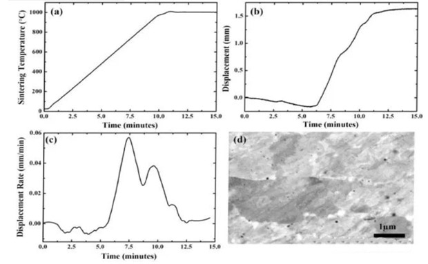
Figure 1. Sintering data of CNA7 atomized powder (a) Temperature-time (b) Displacement-time (c) Displacement rate (d) SEM micrograph of SNA7 sample.
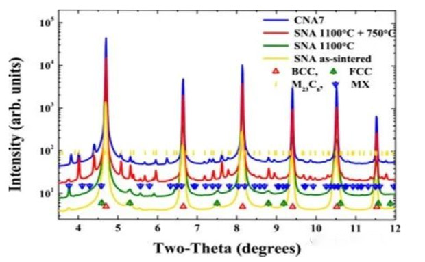
Figure 2 shows the XRD patterns of sintered SNA, solution (1100°C), solution+tempered (750°C) and CNA7 specimens, with phases superimposed for reference. The BCC phase dominates the XRD pattern, and a small amount of FCC austenite and MX components can be seen in both the sintered and solid solution samples. After tempering (red trace in Figure 2), the FCC phase completely disappears, the MC236 phase grows significantly, and the peak position of the M23C6 phase in Figure 2 is superimposed into a triangular vertical line. The change in peak width of the BCC matrix after tempering indicates that tempering effectively eliminates two-dimensional defects (such as dislocations). Comparing the patterns after sintering and tempering, the changes are most obvious at high two-theta angles.
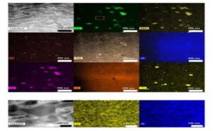
To investigate the chemical composition of the matrix, MX and MC236 precipitates in more detail, STEM-EDS spectra were combined with synchrotron radiation nano-X-ray imaging. Figure 3(a) shows a STEM-EDS micrograph of a representative area of the tempered specimen. The separation of chromium-tungsten-manganese, titanium-vanadium-tantalum and O is very obvious, which proves that there are obvious multiple MX precipitation distributions, both coarse and fine. The high-magnification image in Figure 3(b) confirms that Ti MX precipitates as small as 7.6 nm are uniformly distributed at a high number density (6.5×10²¹ m−3). Representative EDS spectra of the matrix, MC236, and MX precipitates are shown in Figure 3(c). EDS confirmed the chemical complexity of MC236 with a chromium-tungsten-manganese composition, which is consistent with STEM-EDS of castable materials reported elsewhere. Figure 4 shows the synchrotron radiation two-dimensional XRF pattern of the tempered sample. Recent studies have shown that this method can both complement TEM and provide unique insights into the atomic structure of precipitates in additively manufactured 316 L stainless steel. The XRF pattern shows the chemical separation of Ti-V and Cr-W, similar to the STEM-EDS results in Figure 3. It is evident from the XANES spectra in Figure 4 that there are differences in the electronic structures of the substituted chromium atoms in the host (BCC XANES) and M C236 (FCC structure). The BCC structure of substituted chromium atoms dispersed in the matrix is similar to the BCC spectrum of the chromium foil reference. The FCC M C236 reference spectrum (yellow trace in Figure 4) is superimposed on the precipitate spectrum, again demonstrating that the atomic environment of the precipitate is perturbed by the additional W, Mn components quantified by STEM-EDS and XRF imaging.
As a prerequisite for considering the use of sintered variants of CNA-based alloys for complex plasma components, the researchers sought to replicate the cast CNA7 alloy, which has excellent creep and radiation resistance. Such microstructures are easily achieved by applying rapid fabrication DC sintering techniques with the help of computational thermodynamics. Through multimodal microstructural characterization and computational thermodynamic analysis of the sintered nanostructured alloy (SNA), it was found that its microstructure and crystal phase are consistent and identical to its castable nanostructured alloy (CNA). The rapid fabrication enabled by the DCS method and the ability to design the final microstructure through post-thermal tempering are evident. It is worth noting that compared with current CNA alloys, a higher density of fine defects can be achieved through this sintering method, which is crucial for its high-temperature creep and irradiation properties. Mechanical properties (including creep and thermophysical properties (thermal conductivity)) and microstructural properties after neutron irradiation are ongoing. These promising results highlight DCS as a viable fabrication route and highlight the future promise of these methods for developing hierarchical structures using SNA materials on sintered CCNZ, an important step towards designing the realistic structures required for future devices.
More about technology please visit zkij.com.